
What is Our Piezo Advantage?
Our piezo experts have collectively over 100 years of experience designing and manufacturing piezoelectric systems. As part of the Mide family, we have a firm understanding of many engineering applications and teams. We love working with our customers to find new and exciting ways to apply piezoelectric technology to solve engineering problems!
Talk to us about engineering a high-value piezo module to integrate into your system - and accelerate your development cycle! Contact.
Our Areas of Expertise
An understanding of piezoelectrics requires an understanding in a variety of areas.
Multilayer Bonding & Cutting
Piezo.com specializes in manufacturing piezoelectric bending and extending elements. A proprietary bonding process and ceramic qualifying program leads to consistent performance, high-strength, thermally stable, void free, multilayer laminations. Advanced cutting techniques produce actuators with dimensional tolerances within ± .001 inch; chip-free edges; non-linear shapes; and contamination free surfaces.
Resonant Devices
Resonant piezoelectric devices are an effective way of achieving high periodic motion at low voltage and power. Products designed to operate at a single frequency require special attention be paid to dimensional uniformity, material consistency, and process control. A careful balance is sought between minimizing strain on the piezoceramic and maximizing the dynamic amplitude. Energy losses due to internal dissipation, external attachments, and output loading are addressed.
Ultrasonic Transducers
Ultrasonics, a special portion of the resonant spectrum, find extensive use over a wide range of application areas. These devices are designed according to the same principles guiding resonant devices. However, additional consideration is given to amplitude, stability, power consumption, overheating, resonance tracking, and electronic drive.
Embedded Electronics
We have a large electronics team that is familiar with the nuances of designing piezo-based systems and specialize in low-power design. We can help consult your team to integrate a piezo into your system design or consider hiring our team to fully design and produce the electronics and firmware needed.
Piezo Protection Advantage
We also have a patented process for packaging or laminating piezoelectric ceramics. Piezoelectrics have many benefits and are used in a host of applications. With their thin form factor, they can;
- Convert mechanical energy (motion) to electrical energy for sensing or energy harvesting
- Converting an electrical signal into motion/force for actuating, such as providing haptic feedback.
However, they have some challenges that our piezo packaging solves:
- Piezos are brittle – packaging adds robustness
- Piezos are difficult to electrically connect to – packaging integrates the electrical connection
- Harsh environments can damage raw piezos – packaging provides a hermetic seal and insulation
- Assembly of raw piezos is labor intensive – packaging eases mechanical integration
- Piezos typically contain lead – packaging reduces the risk of lead exposure
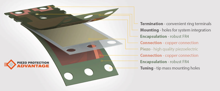
How Does the Packaging Work?
The exploded view graphic (above) illustrates a PPA uni-morph configuration (bi-morph and quad-morph are also available) where piezo wafers are sandwiched between thin, flexible circuits. Piezo.com typically uses either FR4 (like those in a standard printed circuit board) or Polyimide for the flex circuits, but any circuit material can theoretically be used.
A layer of high-temperature polysulfone plastic is used to align the piezo wafers to the copper connections in the flex circuits. The flex circuit then runs the piezo connection out to a convenient electrical termination (connector or solder pads). Finally, a high-temperature epoxy is used to adhere all the layers together in the packaging process to encapsulate the high-performance piezo ceramics between copper-clad insulating materials creating a robust, hermetically sealed, electrically insulated transducer with easy connection.
5 Benefits of Packaging Piezos
1. Packaging Adds Robustness
The most common piezoelectric materials are ceramics. Ceramics are very strong and stiff under tension, but they are also very brittle and susceptible to cracks. Piezo.com’s packaging process solves this problem by sandwiching the ceramic between layers of polymers to form a composite, which distributes strain throughout and therefore reducing the likelihood of cracks in the ceramic. A simple drop or light tap of a raw piezoelectric wafer will crack it; this won’t happen with Piezo.com’s packaging.
2. Packaging Integrates the Electrical Connection
Piezo.com packages the raw piezoelectric ceramic between layers of flexible circuits (typically either FR4 or Polyimide); these are similar to the layers that are found in a standard printed circuit board. As such, there are electric connections that can run throughout the layer and directly connect an external solder pad or connector to the piezoelectric wafer. With a standard piezoelectric ceramic, the user needs to use solder which is notoriously difficult to adhere to these ceramics or a conductive epoxy which can be unreliable.
3. Packaging Provides a Hermetic Seal and Insulation
Raw piezoelectric wafers can’t be exposed to the environment. Water moisture in the air will pose a real danger of damaging the piezo or compromising the electrical connection. Excessive dust can also slowly wear away the ceramic and especially the thin electroding layer on the outside of the piezo. Piezo.com’s packaging completely seals and insulates the raw wafer to enable its use in any environment, even fully submerged in water!
4. Packaging Eases Mechanical Integration
Piezo ceramics are difficult to integrate or assemble into a mechanical system. Not only are they brittle; but they typically come in rectangular or circular shapes with very little opportunity for the inclusion of mounting features. A packaged piezo can easily include holes and other custom shapes to better integrate into your system.